Comparison of All ZKP Hardware Companies
In this research article, these topics will be discussed:
In this research article, these topics will be discussed:
ZKP definition
Why are ZKPs slow and why do we need to accelerate them?
ZKP Algorithms
Hardware used to accelerate ZKP
A List and Comparison of GPU Companies
A List and Comparison of FPGA Companies
Why is ASIC not important for ZKP at the moment? & A List of ASIC Companies
Introduction
Privacy and security are paramount in a blockchain, and these two things seem lacking in view of recent developments in blockchain technology over the past few years. Well, there’s a solution and this solution is relatively new and being explored by various teams trying to accelerate its development to hasten its use in our technology today. This solution won’t only improve blockchain technology but also technology at large.
What’s this solution you’re talking about?
Well, it’s ZKP.
What’s ZKP?
ZKP stands for Zero Knowledge Proof. Just as it connotes, it means having zero knowledge of a proof (data). For data to be safe and private, the second party (verifier) mustn’t know the details of the proof or data. So, ZKP is a computational protocol that a prover (first party) uses to convince the second party that certain data is true without revealing the data. Unlike current web protocols, which require you to provide data to prove its authenticity, ZKP technology does not require you to do so; boom, your data is safe and secure with ZKP technology.
However, the way we are generating ZKP is now slow and expensive, because encrypted algorithms are complicated and it takes a lot of time to hash with the current level of hardware we have, and the equipment (hardware) are expensive (in terms of purchasing costs, hash -> unit cost per hash, cost-effectiveness, etc)
The good news is, there are hardware components (GPU, FPGAs, ASIC) that can accelerate ZKP faster; although most are expensive. This will foster the adoption of ZK proving where individuals will use this hardware to mine proofs in a bid to get compensated, similar to bitcoin mining.
Why are ZKPs slow and why do we need to accelerate them?
Proving a computation requires a prover to convert a proof from a classical program to a Zk-friendly program. This can be done by converting a code to a high-level language like Cairo or Circom, which compiles it down to generate a proof. Most computations aren’t Zk-friendly, which makes proof generation longer as well as more complex and expensive operation. However, once a proof is in Zk format, it’s sent to a proof system: ZK-snark, ZK-stark, etc (they’re other Zk algorithms like Plonk, Spartan but these are the two most popular), where Zk-friendly computations are outputted as proofs.
Let’s talk about these ZKP algorithms.
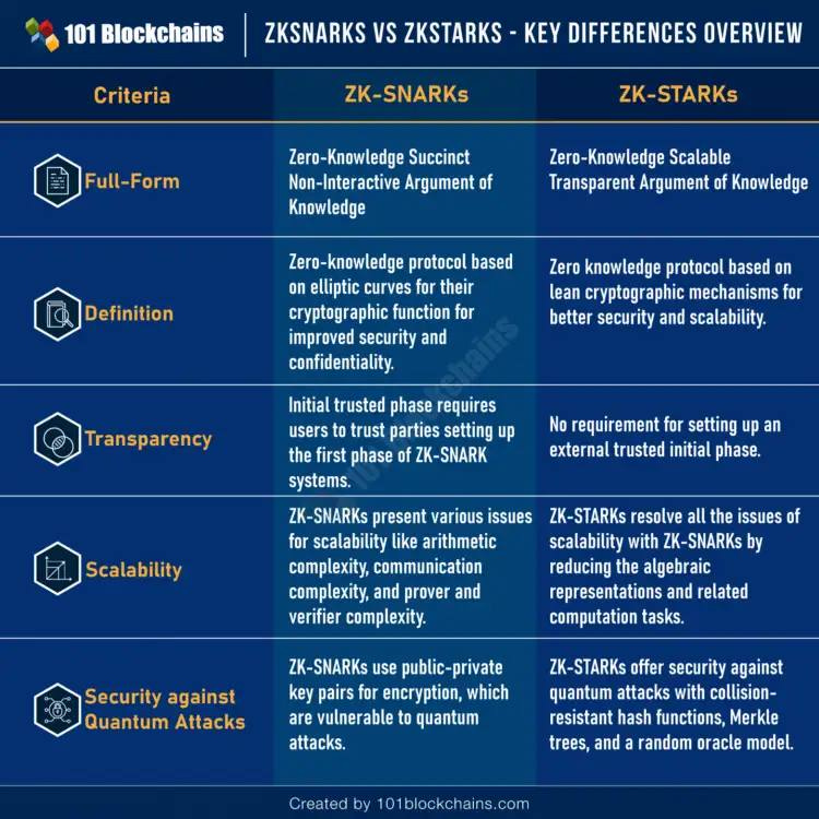
ZK-snark vs Zk-stark
Zksnark (Zero-Knowledge Succinct Non-interactive Arguments of Knowledge) is a ZK option for elevating security in ZK tech. It uses an elliptic curve design for its effectiveness. The word “succinct” implies a smaller size of proofs and quick verification, while “non-interactive” means no interaction between the prover and verifier. The Argument of Knowledge means the honesty of the computation by the prover. A prover would have to provide an argument of knowledge to support his statement, or else the prover becomes dishonest.
ZKstark (Zero-Knowledge Scalable Transparent Argument of Knowledge) This was invented by Starkware in 2018 to improve hashing (identifying an object from a group) in cryptography. You can deduce its functions from its full name — “Scalable” means the ability to handle larger proof-size in a short period; Transparent: ZK-stark doesn’t need any initial trusted setup; this describes it as being transparent.
Both algorithms of ZKP are building towards the same goal. However, it’s important to note that both have key differences. ZK-stark provides more scalability, transparency, and security for blockchains than Zk-snark, although it has a larger proof size and takes a long time to verify proofs.
Even though Starks have a positive light here, Snarks still seem to be better because they create proofs that are a few hundred bytes long, making it easy to verify the proofs and also faster, giving them an upper hand over Starks.
The verification cost for Snarks and Starks can vary. Snark proofs cost 290,000 gas to verify Eth, while Stark proofs cost 5 million gas.
It’s important to note that there are bottlenecks in a proof system. These bottlenecks are FFT (Fast Fourier Transforms) and MSM (Multi-Scalar Multiplication). Both are algorithms and are slow to prove generation. But, ‘PipeZK’ is a way to address the MSM-FFT issue using Pippenger’s algorithm to make MSM cheaper and another method to ‘unroll’ FFTs.
Suppose these methods help address bottleneck issues in ZKP. What hardware accelerates this process?
Hardware Used to Accelerate ZKP
There are 3 known hardware technologies used to accelerate ZKP. These include GPUs, FPGAs, and ASICs.
FPGA (Field Programmable Gate Array): These are chips or semiconductor devices programmed to do almost any digital function. It can be configured by a customer to perform any purpose favorable to the customer.
GPU (Graphics Processing Unit): These are chips that can process many pieces of data simultaneously in a machine. It was initially designed for graphics, but its parallel structure makes it able to handle super computation and also mining.
ASIC (Application Specific Integrated Circuit): Just as its full meaning implies, it’s a chip used for specific purposes, mostly used to mine cryptocurrency; and it’s not crypto-specific.
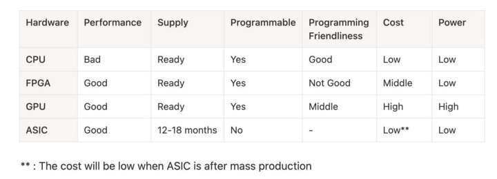
Comparison of these hardware components
From the table above, we can see that FPGA is a preferable hardware choice from the developer’s perspective. CPUs aren’t used because of its poor performance and incapability for ZKP computation. ASIC is the miner’s choice. Once the ZKP mining industry commences, ASIC will become very important. This can take a number of years from now to happen.
A List and Comparison of GPU Companies
GPU
The two biggest names in GPU production are Nvidia (NVDA) and Advanced Micro Devices (AMD), with Intel coming in behind.
Nvidia (NVDA)
It was the first company in the world to manufacture a GPU in 1999, named GeForce 256; it also launched its IPO (Initial Public Offering) at $12 per share that same year. It has a market cap of $302.504 billion and controls 10% of the GPU market share.
According to the website, “8 of the world’s top 10 supercomputers use NVIDIA GPUs, InfiniBand networking, or both. NVIDIA powers 346 of the overall Top 500 systems on the latest list.” NVIDIA boasts the world’s fastest industrial supercomputer — Selene, ranked 5 in the world
Its latest GPU product is the GeForce RTX3090, which costs $1499 and is the best GPU product at the moment.
Advanced Micro Devices (AMD)
Started as a startup in Silicon Valley in 1969, it has since developed to become one of the most trusted producers of GPUs. It entered the GPU market in 2006 after acquiring leading video card maker ATI for $5.6 billion, with $4.2 billion in cash and $1.2 billion in stock. AMD has a market cap of $102.283 billion and has shipped over 500 million GPUs since 2013.
Its latest GPU product is the AMD Radeon RX6000.
Intel
By revenue, Intel is the world’s largest semiconductor chip manufacturer. It has a hub of products like central processing units, microprocessors, and many more, but, most notably in this article, the Integrated Graphics Processing Unit (iGPU) is one of its products that manufactures GPUs.
It’s set to launch two products, Arc A770 and A750, on October 12th. The A770 will start at $329, while the A750 will be at $289. Intel claims these products will be better than GeForce RTX.
Comparison of Arc A770 and A750
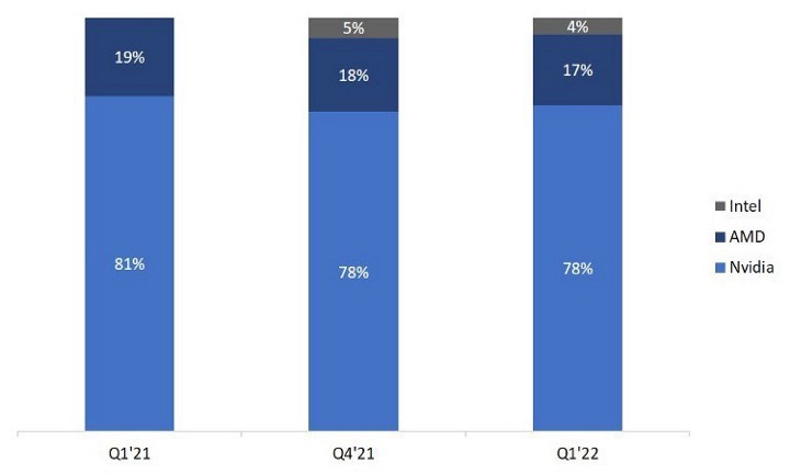
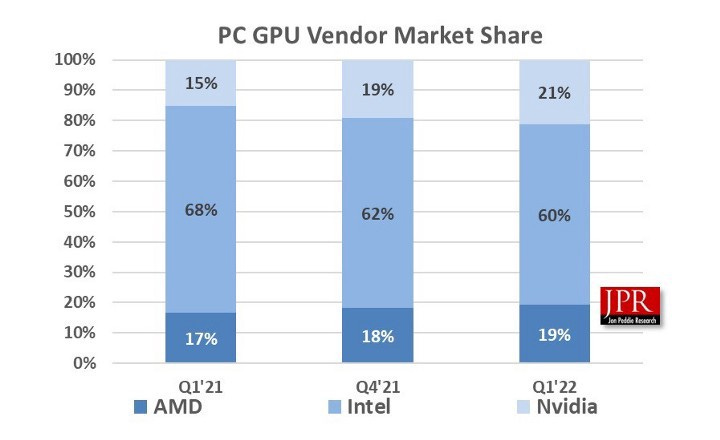
GPU Market Share
A List and Comparison of FPGA companies
FPGA
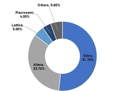
At least 5 companies are making FPGAs in the world currently. These include Xilinx, Altera, Lattice, Actel, and QuickLogic. The first two are the biggest names in FPGA, and they hold the bulk of the market. whereas the latter 3-Lattice, Actel, and QuickLogic are small players. A notable mention is QuickLogic.
Xilinx
Founded in 1984, it became the inventor of FPGA. Its philosophy revolves around being transparent (i.e. open about its device architecture) and providing lots of useful features and complex tech.
In 2022, tech giant AMD completed the payment of $49 billion to acquire Xilinx. It’s now called AMD Xilinx. Its latest product is the Xilinx VU9P board which costs $8394.
PCle Gen3 X 16.
Xilinx Virtex Ultra Scale and VU9 FPGA
Two QSFP28 optical cages for multi-networking solutions
Onboard two DDR4 and two QDR2 and sign independent banks.
Fall safe configuration
Tandem configuration mode available
JTAG connector
Altera
Altera focuses on ease of usage and functions, with very good HDL software. It was founded in 1983 by semiconductor veterans-Robert Hartmann, James Sansbury, Rodney Smith, and Paul Newhagen with a seed money of $500,000. The company had a long-running design partnership with the tech giant, Intel.
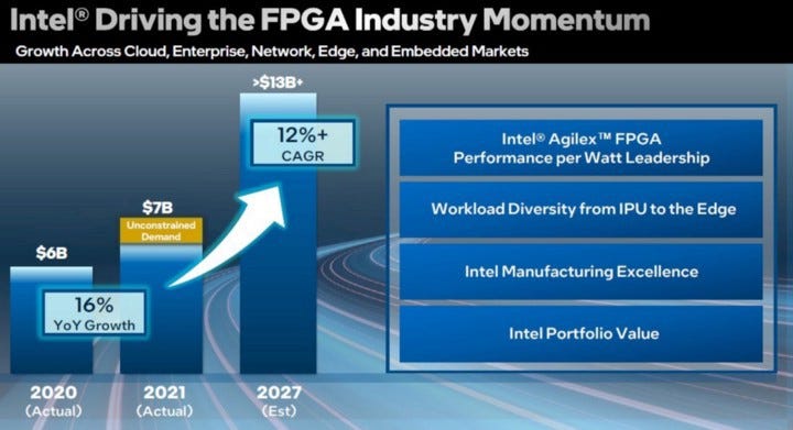
Interestingly, Intel spent $16.7 billion to acquire Altera in 2015. Back then, Intel was very concerned about their competitor Nvidia getting a monopoly over the FPGA market, having experienced an incredible near-monopoly from the X86 datacenter. Intel felt the need to get a chunk of the FPGA market share.
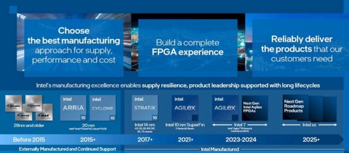
Its latest product is the Intel Agilex F-series.
Differences between Xilinx and Altera FPGAs
The main difference between Xilinx and Altera is that Xilinx is mainly for application development purposes. Altera’s FPGAs are essential for industrial design and embedded applications. Due to the popularity of Xilinx devices, many tools support Xilinx devices.
PLI (Protocol Level Interconnect) is Altera’s native communication, which helps in the communication of IP blocks between devices. It offers different and effective communication between IP blocks. While Xilinx series FPGA boards use the IEEE 1394 interface (an interface standard for high-speed communication and isochronous data transfer).
Free SDK and programmable logic design tools — Altium Designer and Quartus 11 — are available for Xilinx series FPGA boards.
Lattice Semi-Conductor
The company was founded in 1983 and has an annual revenue of more than $400 million as of 2019. Its headquarters are in the Silicon Forest area of Hillsboro, Oregon.
It specializes in the design and manufacturing of low-power FPGAs. Its FPGA product is the Lattice Mach X05-NX family.
Mach X05-NX Family
This is the fifth device built on the Lattice Nexus platform. Mach X05-NX enables the latest generation of secure control through 3.3 V I/O support, increased logic and memory resources, and a differentiated security feature set.
Features
Increased logic and memory resources
It combines a 25k logic cell capacity FPGA fabric with 1.9 MB of embedded memory to reduce the design footprint. This is done by minimizing the need for external memory. It also offers 9.2MB of dedicated user flash memory to store mission-critical data.
It also enables a single chip solution that supports multiple configuration images thanks to its instant-on operation and reliable in-feed updates.
Thanks to the added DSP and ADC blocks, It offers greater computer and control capabilities.
Security leader
It has an on-chip multi-boot with bitstream encryption (AES256) and authentication (ECC256).
It has an advantage over FPGAs of a similar class, which is run-time security.
Power Efficiency and Reliability Leader
Devices built on the lattice Nexus platform deliver up to 70% more than competing FPGAs of similar devices.
The FD-SOI manufacturing process contributes to a 100-fold lower soft error rate and improved system reliability compared to other FPGAs in the same class.
Actel
It was a manufacturer of non-volatile, low-FPGAs, mixed-signal FPGAs, and programmable logic solutions. Its headquarters were in Mountain View, California. Actel was acquired by Microsemi in November 2010, in a deal worth $430 million.
Microsemi-Corporation was located in Aliso Viejo, California. It was a provider of semiconductors and system solutions for data centers, aerospace, defense, industrial markets, and communication. It was acquired by Microchip Technology in a deal worth $10 billion in May 2018.
Microchip Technology is an American company that manufactures microcontrollers, analog, mixed-signal, and flash-IP integrated circuits. It has a revenue of $8 billion.
Product
It has a wide range of FPGA families that aid in each respective purpose: high speed, high security, or high volume. Microchip Tech has FPGAs for each integration need.
PolarFire Mid-Range FPGA
This combined low cost and SerDes and DSP abs resources to produce a range of high-speed and compute-intensive systems.
a) the most cost-effective and power-efficient in their class
b) highest level of security and dependability
c) Transceivers ranging from 250 Mbps to 12.7 Gbps
d) 33 MB of RAM and 100k to 500k logic elements
IGLOO 2 Low-Density FPGA
This FPGA gives more resources than other FPGAs, and it improves design integration. This FPGA is ideal for a variety of applications due to its security, low power consumption, and reliability.
a) Consumes ~50% less power than comparable FPGAs
b) non-volatile
c) instant start
d) PCIe Gen 2 support in devices as low as 10K LE
ProASIC 3 FPGA
If you’re designing around an Arm Cortex-M1 processor, then this FPGA should be your choice for a better result.
a) Comes with arm enabled processor
b) low power devices up to 35k logic element
c) is equipped with flash-freeze technology
IGLOO FPGAs
This FPGA identified itself as:
a) Can be used in place of a CPLD (Complex Programmable Logic Device).
b) For CPLD applications.
c) FPGA with low density
d) It is equipped with an Arm Cortex-M1 processor core and flash-freeze technology.
Fusion Mixed Signal FPGA
This FPGA integrated both analog and digital functions into its chip. It includes, as follows: configurable analog, powerful clock generation, and high-performance flash-based programmable logic.
a) Compatibility with the following microcontroller cores: Arm Cortex-M1, 8051, and CoreABC
b) ADC (Analog to Digital Converter) and circuit maintenance — monitoring voltage, current, and temperature.
c) ProASIC 3 FPGA fabric with ~ 1.5M gates and 292 analog and digital I/Os
Quick Logic
This is a fabless semiconductor company. It develops low-power multi-core semiconductor platforms and intellectual property for AI. It was founded in 1988, its headquarters are in San Jose, California. It has a market cap of $84.80 million.
Quick Logic develops a full-stack platform for artificial intelligence (AI), voice, and sensor processing. Its products include primarily FPGA families named pASIC3 and QuickRAM, as well as programming hardware and design software. It also has an IP business that licenses its eFPGA technology for use in other semiconductor companies’ SoCs.
Recently, on Sept. 8, 2022, it was awarded a $6.9 million base contract to develop and demonstrate Strategic Radiation Hardened (SRH), high-reliability Field Programmable Gate Array (FPGA) technology to support identified and future Department of Defense (DoD) strategic and space system requirements.
This project is sponsored by DoD’s Trusted and Assured Microelectronics (T&AM) Program and Naval Surface Warfare Center (NSWC) Crane, the government’s technical lead.
Brain Faith, the president of QuickLogic, had this to say: “QuickLogic is honored to have been chosen by the US Government to lead this highly specialized and mission-critical program. This project builds on the company’s 30+ year heritage of delivering FPGA technology to the Aerospace and Defense community while operating in some of the most rugged environments.”
QuickLogic will collaborate with a team composed of SkyWater Technologies, Everspin Technologies, and Trusted Semiconductor Solutions to lead this execution.
At the discretion of the US government, upon the success of this project, the contract allows for options totaling ~$72 million over multiple years.
Product
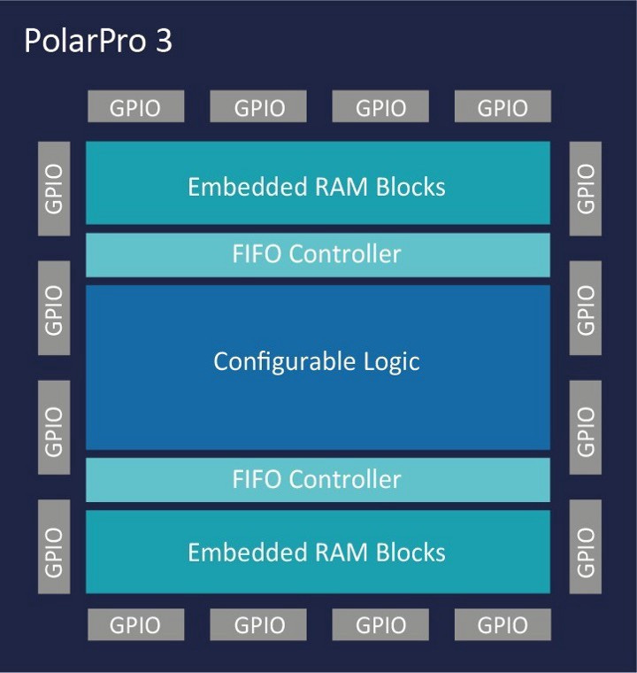
QuickLogic announced PolarPro 3, a tiny, low-cost SRAM programmable FPGA with Open Source Tools, on February 10, 2022. It consumes power at as low as 55 uA and has a tiny size too; making this product flexible and less- energy-consuming.
In it, there are 2,000 effective logic cells of SRAM-based FPGA fabric, up to 46 configurable I/Os, and 64Kbits of SRAM.
Due to its lower energy consumption and flexibility, the PolarPro 3 becomes family-friendly, very mobile, and wearable.
Accessibility
It’s accessible to a wide range of users due to support from QuickLogic’s tool suite, open-source tools such as Yosys Open Synthesis Suite.
Benefit
Through the use of small chips, this tech solves the most challenging embedded systems architecture challenges. Connectivity, system latency, system power consumption, and time-to-market.
Features
Reprogrammable SRAM technology.
RAMs are integrated using dedicated FIFO controllers embedded in each block.
supported by open-source FPGA tools
Use Cases
interface to a different bus or IO voltage
Bus interfaces: MCU to memory, MCU to MCU, MCU to peripherals/displays/I2C/I2S/SPI/UART/PWM
List of ASIC Companies and Why is ASIC not important for ZKP at the moment?
ASIC
In this article, ASIC won’t be talked about much because ASIC is not only used in crypto / for ZKP and I believe it’ll take some time for full-fledged mining activity on ZKP tech.
Well, without a doubt, ASIC is a very important ZKP tool in the long run, even though the POW sentiments and not being environmentally friendly are a big hindrance for mining nowadays.
An ASIC (Application Specific Integrated Circuit) is a chip customized and made for a particular purpose instead of a general purpose.
All ASICs are tailored to mine-specific algorithms. This means ASICs made for bitcoin algorithms will only work on cryptocurrencies that use the same algorithm as bitcoin.
Companies Manufacturing ASIC
Reports say that the global ASIC chip market was valued at $18.51 billion in 2020 and is expected to grow at a CAGR (Compound Annual Growth Rate) of 9.73% from 2021 to 2028, reaching $35.44 million by 2028.
Just as we saw in some cases in the GPU and FPGA markets, some key market players buy out competitors to gain significant market share to stay on top, the ASIC market is no different. Companies holding the top market share in ASIC include
Bitmain Technologies, Ltd.
Infineon technologies
Intel Corporation
Nvidia Corporation
Samsung Electronics Co., Ltd.
Taiwan semiconductor manufacturing
Texas Instruments
Xilinx, inc., now AMD Xilinx
On semiconductor now Onsemi group
Advanced Micro Devices, Inc.
These are the major players in the ASIC market.
Conclusion
In general, we can see some patterns in each hardware market. The big boys swallow the little ones to become bigger at an amicable transaction deal.
Well, it’s healthy competition as each big company wants to get ahold of the market share, and you can’t win a market share without winning the customer’s heart and improving technology. This will breed healthy competition toward making a better technology, thereby accelerating ZKPs and getting a market share. It’s a win-win situation for everyone.
SOURCES:
https://www.paradigm.xyz/2022/04/zk-hardware
https://www.microsoft.com/en-us/research/uploads/prod/2021/05/isca21_pizk-60a269dbb1310.pdf#page12
https://hackernoon.com/using-cloud-zk-for-developing-zkp-acceleration-in-the-cloud
https://101blockchains.com/zksnarks-vs-zkstarks/
https://www.investopedia.com/terms/g/graphics-processing-unit-gpu.asp
https://www.investopedia.com/news/amd-versus-nvdia-amd-nvda/
https://en.m.wikipedia.org/wiki/Nvidia
https://www.tomshardware.com/features/amd-vs-nvidia-gpus
https://medium.com/amber-group/need-for-speed-zero-knowledge-1e29d4a82fcd
https://en.m.wikipedia.org/wiki/Intel_Graphics_Technology
https://trapdoortech.medium.com/zero-knowledge-proof-fpga-or-gpu-97b96ffbf0f
https://www.fpga4fun.com/FPGAinfo1.html
https://www.raypcb.com/xilinx-fpga-vs-altera-fpga/
https://www.nextplatform.com/2022/09/27/intel-to-broaden-fpga-lineup-and-make-them-at-home/amp/
https://en.m.wikipedia.org/wiki/Xilinx
https://en.m.wikipedia.org/wiki/Field-programmable_gate_array
https://en.m.wikipedia.org/wiki/Altera
https://www.intel.com/content/www/us/en/products/details/fpga.html
https://www.intel.com/content/www/us/en/products/details/fpga/agilex/f-series.html
https://en.m.wikipedia.org/wiki/Lattice_Semiconductor
https://www.microchip.com/en-us/products/fpgas-and-plds/fpgas
https://www.reuters.com/markets/companies/QUIK.A/


